How many PINs are there in 8086? | Symbols, Types, and Functions.
 |
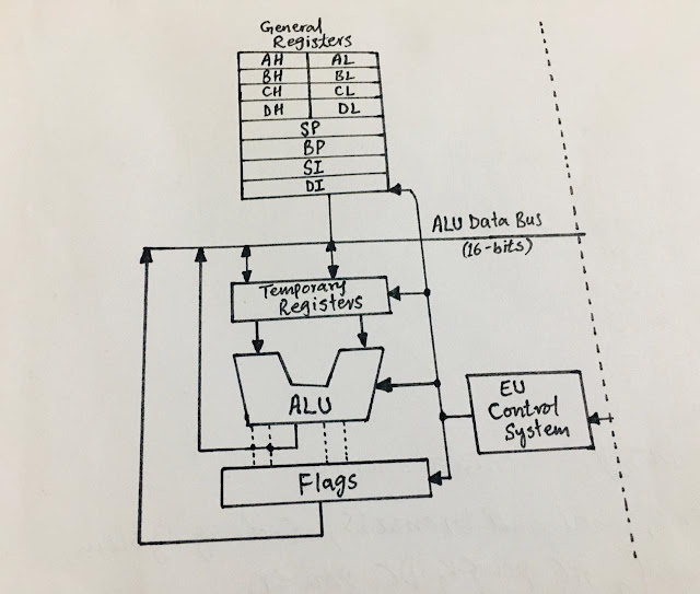
| 8086 Pins |
8086 Pins:
Of the 40 pins or anchors, 32 anchors have the same functions in low or high mode, the remaining 8 anchors have different functions in low and high mode. The 8086 anchors are the basic symbols of a system bus and can be divided into three types;
• 16 bits data buses: D15-D0
• 20-bit address bus: A19-D0
• Control bus: ALE, Memory I / O (M / IO), WR, RD, OK, INTR, INTA, NMI, HOLD, HOLDA, RESET, CLK, Vcc, GND.
The 8086 is a 16-bit microprocessor that connects to the outside world via a 16-bit data bus, which requires 8086 to undergo a single reading cycle to download 16-bit data.
The 8086's 20-bit address bus can have up to 1 MB of memory (2020 = 1,048,576 B, to be exact).
Main Functions of 8086 Pins:
The main functions of the 42 8086 microprocessor pins are to
provide control signals that allow external rotation to take over 8086 buses.
Two distortion lines are included to provide the ability to distort the mask
can be seen and invisible.
Multiple status results are available, which are used to
determine any internal CPU regions.
Some control signals are provided to allow interaction with
other interference.
Output or input will be completed with nails.
The 8086 has two efficient modes for working low mode and high mode (large mode). Anchors in the processor are designed for two
purposes, one for the minimum and the other for the advanced mode. Common
markers or pins are present both high and low.
|
Common Signals |
||
|
NAME |
FUNCTION |
TYPE |
|
AD15_AD0 |
Address/data bus |
Bidirectional, 3-state |
|
A19/S6-A16/S3 |
Address/status |
Output, 3-state |
|
MN/MX |
Min-max mode control |
Input |
|
RD WR |
Read control |
Output, 3-state |
|
TEST |
Wait on test control |
Input |
|
READY |
Wait for state control |
Input |
|
RESET |
System reset |
Input |
|
NMI |
Non maskable interrupt request |
Input |
|
INTR |
Interrupt request |
Input |
|
CLK |
System clock |
Input |
|
Vcc |
+5V |
Input |
|
GND |
Ground |
|
Pins for the Minimum mode:
|
Minimum mode signals 1(MN/MX=Vcc) |
||
|
NAME |
FUNCTION |
TYPE |
|
HOLD HLDA WR M/IO DT/R DEN ALE INTA |
Hold request Hold acknowledge Write control Memory/IO control Data transmit/receive Data enable Address latch enable Interrupt acknowledge |
Input Output Output, 3-state Output, 3-state Output, 3-state Output, 3-state Output Output |
Pins for Maximum mode:
|
Maximum
mode signals (MN/MX=GND) |
||
|
NAME |
FUNCTION |
TYPE |
|
RQ/GT LOCK S2-S0 QS0, QS1 |
Request/grant bus Access control Bus priority lock control Bus cycle status Instruction queue status |
Bidirectional Output, 3-state Output, 3-state Output |
Symbols, PIN numbers, and their respective functions:
 |
| Pins with numbers |
• Pin No: 39, 2-16
• Type: I / O
• AD bus: multiplexed memory / IO address (T1), and data
(T2, T3, Tw, T4) bus.
These lines operate HIGH and the float goes to 3-state OFF
during the interruption of the reception and the local bus "hold
hold".
• Symbol: A19 / S6, A18 / S5, A17 / S4, A16 / S3
• Pin No: 35 - 38
• Type: O
• Address/line status
• T1 time: address and then between T2, T3, Tw, T4 status
• S5: IF flag status and S6: DOWN
Symbol: BHE # / S7,
Pin No: 34,
Type: Oh,
• High Bus Allow / Status
Symbol: MN / MX #
• Pin No: 33
• Type I
• Minimum / Size: indicates which processor to work with.
HIGH shows low mode (single processor system)
LOW displays high mode (Multi-processor system).
Symbol: RD #
• Pin No: 32
• Type: O
• Read: RD works LOW during the learning cycle on T2, T3,
and Tw clocks and shows that the processor makes a memory or read I / O.
Symbol: TEST #
• Pin No: 23
• Type: Me
• Test: input checked the 'wait' command if TEST #
processor LOW will continue to perform otherwise wait in idle mode. This
installation is synced internally during each clock cycle on the leading edge
of the CLK.
• Symbol: OK
• Pin No: 22
• Type: Me
• Fixed: Ready signal is obtained from memory or I / O
devices to indicate complete data transfer. EASY is often used to synchronize a
fast processor with slow memory or with an I / O device that may require
additional bus cycles to perform reading or writing tasks. Synced by 8284
generator clock.
Symbol: NMI (Non-Hidden Interference)
• Pin No: 17
·
Type: I
·
NMI: not influenced by the interrupt enable flag
(IF), not maskable internally by software requires a rising edge to be recognized,
and it cannot be internally disabled (masked) by software.
NMI was adopted by 8086 at the end of the
current order.
·
The address of type 2 ISR (disruption of
operation) is read in the table containing the full ISR address.
• Symbol: RESET
• Pin No: 21
• Type: Me
• Reset: input causes the
processor to quickly disconnect its current function. Must be at least 4 clock
cycles.
A high level of intelligence is
required to activate the installation of RESET, which must remain at least four
clock cycles to ensure proper operation.
Reset the signal that activates
the processor after activation. The reset can be used during the program and
the type of panic button used to start the program from the beginning.
• Symbol: CLK
• Pin No: 19
• Type: Me
• Clock: provides basic processor
time and bus control. It is equivalent to a 33% work cycle to provide a
well-designed internal time. A 33% work cycle means that the digital rate is
one-third of the time.
CLK input requires a digital
digital form with a 33 percent work cycle.
• Symbol: INTR
• Pin No: 18
• Type: Me
• Interrupted Request: If the INTR
are the 1st point during the last command clock cycle and the interfering flag
(IF) has 1 point, the 8086 microprocessor will enter the interrupt
acknowledgment function after performing the current teaching function.
Samples at the last hour of each
teaching cycle.
The INTR type of interference is
actually read in the processor data bus during a known disruption cycle.
• Symbol: Vcc
• Pin No: 40
• Vcc: + 5V power supply pin
• Symbol: GND
• Pin No: 1,20
• EARTH
Symbol: DT / R #
• Pin No: 27
• Type: O
• Transfer Data / Receive
DT / R is an output that is used
to control the flow of data on the 8286/887 data bus transceiver. When DT / r
is low, data should flow to 8086, while DT / R is high, 8086 output data.
Logically DT / R is equal to S1 in
high mode, and its duration is the same as that of M / IO. DT / R floats too
high impedance on the local bus "hold appro".
Symbol: DEN # (Enable Data)
• Pin No: 26
•Type: I
• DEN:
Symbol: Latch Address Enabled
(ALE)
• Pin No: 25
• Type: O
• ALE: is the highest active beat
between T1 of any bus cycle. Provided an address entry processor for the
address latch of 8282/8283.
Symbol: M / IO #
• Pin No: 28
• Type: O
• Status Line: used to separate
memory access for I / O access. High for memory performance and LOW I / O
performance.
·
Symbol: WR #
·
Pin No: 29
·
Type: O
·
Write: indicates that the processor is
performing write memory or write I/O cycle.
Symbol: INTA # (Approval of Approval)
• Pin No: 24
• Type: O
• INTA: used as a study strobe to disrupt consent cycles.
LOW active during T2, T3, and Tw for each cycle acceptance disturbance.
• Symbol: HOLD, HLDA
• Pin No: 31, 30
• Type: Me, O
• Catch: indicates that another chief is asking for a local
bus to "catch". The processor that receives the “hold” request will
issue HLDA (HIGH) as approved.
Symbol: S2 #, S1 #, S0 #
• Pin No: 26-28
• Type: O
Status: active between T4, T1, and T2and is restored
automatically (1, 1, and 1) between T3 or Tw when READY IS HIGH. 8288 Bus
Controller used to generate all memory and signals to control access.
Symbol: RQ # (Application) / GT0 # (Grant), RQ # / GT1 #
• Pin No: 30, 31
• Type: I / O
• RQ / GT: anchors are used by some local masters to force a
processor to release a local bus at the end of the current processor bus cycle.
RQ / GT0 # is more advanced than RQ / GT1 #.
Symbol: Lock #
• Pin No: 29
• Type: O
• Lock: output indicates that some system bus managers
should not get control of the system bus while LOCK is operating LOW. The
prefix “LOCK” is applied and remains active until the next command is
completed.
• Symbol: QS1, QS0
• Pin No: 24, 25
• Type: O
• Line Status: Line mode is applied during the CLK cycle
after linear action.

Comments
Post a Comment
if you have any doubt, please let me know.